










How to Measure Both Thickness and Shape of Transparent Materials: SinceVision Spectral Confocal Displacement Sensor Technical Guide
SinceVision SCI04025 spectral confocal displacement sensor measures transparent material thickness and 3D surface shape simultaneously in a single non-contact pass using wavelength-encoded axial dispersion. By isolating dual reflection peaks from upper and lower boundary interfaces, it delivers 0.06 μm static repeatability and ±0.8 μm linearity across battery cold plates, semiconductor wafers, and precision optical components.
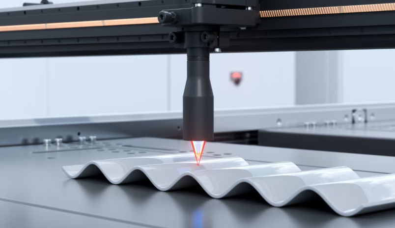


A spectral confocal displacement sensor measures transparent material thickness and 3D surface topography simultaneously in a single probe pass. By projecting polychromatic light through an optical pen that focuses different wavelengths at distinct depths along the vertical axis, the SinceVision SCI04025 identifies reflection peaks from both the upper (air-to-coating) and lower (coating-to-substrate) boundaries. The sensor captures surface elevation and calculates true layer thickness through non-contact height difference detection with sub-micron repeatability.
Quick Reference: SinceVision SCI04025 Technical Specifications
| Parameter | Specification | Engineering Function | Quality Defect Prevented |
| Measurement Technology | Spectral confocal displacement sensing | Wavelength-encoded axial depth recognition | False height readings caused by refractive beam splitting |
| Linearity | ±0.8 μm | Absolute dimensional accuracy across measurement range | Cumulative profile errors during 3D topography mapping |
| Static Measurement Repeatability | 0.06 μm | High-precision stability for quality verification | Misclassification of borderline parts in statistical process control |
| Minimum Measurable Thickness | 130 μm (for transparent objects) | Discrete boundary peak resolution | Peak overlap causing unmeasurable thin-film regions |
| Optical Working Distance (Standoff) | 16 mm | Generous clearance for station integration | Probe collisions with warped surfaces or moving assembly tooling |
| Measurement Mode | Non-contact optical sensing | Eliminates mechanical contact force and tip wear | Surface scratching, coating deformation, and substrate damage |
1. What Makes Testing Corrugated Surfaces and Transparent Materials Challenging?
Inspecting transparent coatings over corrugated metal surfaces presents a dual optical challenge: sensors must simultaneously profile the physical waviness of the substrate and identify two closely spaced optical boundary reflections. Conventional sensors fail because light penetrates the transparent coating, creating multiple overlapping reflections and refractive beam bending that distort surface elevation and thickness calculations.
The Inspection Problem on EV Battery Water-Cooled Plates
In new energy vehicle (NEV) and electric vehicle (EV) battery packs, water-cooled cold plates serve as critical thermal management components. The aluminum plates feature corrugated channel structures designed to circulate coolant beneath the battery cells. To ensure electrical safety, a protective dielectric insulation coating is applied across these corrugated profiles.
This manufacturing process introduces two competing quality requirements:
Insulation Protection: The coating must maintain a uniform thickness to prevent dielectric breakdown and high-voltage electrical arcing between the battery cells and the aluminum plate.
Thermal Dissipation: Excessive coating thickness creates thermal resistance, trapping heat inside the battery pack and compromising overall product reliability.
Accurately measuring film thickness and detecting thickness deviations in real time are mandatory steps in cold plate quality control.
The Metrology Challenge: Dual-Interface Recognition
The insulating coating applied to water-cooled plates is typically transparent or translucent. During inspection, a sensor must execute two separate tasks simultaneously:
Measure the absolute 3D surface elevation and shape of the corrugated coating profile.
Accurately identify the spatial positions of both the top surface (air-to-coating interface) and the bottom surface (coating-to-substrate interface).
If an optical sensor cannot isolate both interfaces, the measurement signal is compromised. The sensor will either track only the metal substrate underneath, blend both reflections into a false average height, or lose signal entirely along the slopes of the corrugated channels.
Testing transparent coatings on corrugated geometries requires high interface recognition capability combined with sub-micron measurement accuracy.
2. Precise Thickness Measurement: Balancing Accuracy and Stability
The SinceVision SCI04025 spectral confocal displacement sensor balances measurement precision and production stability by using axial chromatic dispersion. The sensor splits white light into a spectrum of focal planes along the Z-axis, isolates dual reflection peaks coaxially through a spatial pinhole, and calculates true film thickness from the calibrated height difference without contacting the workpiece.
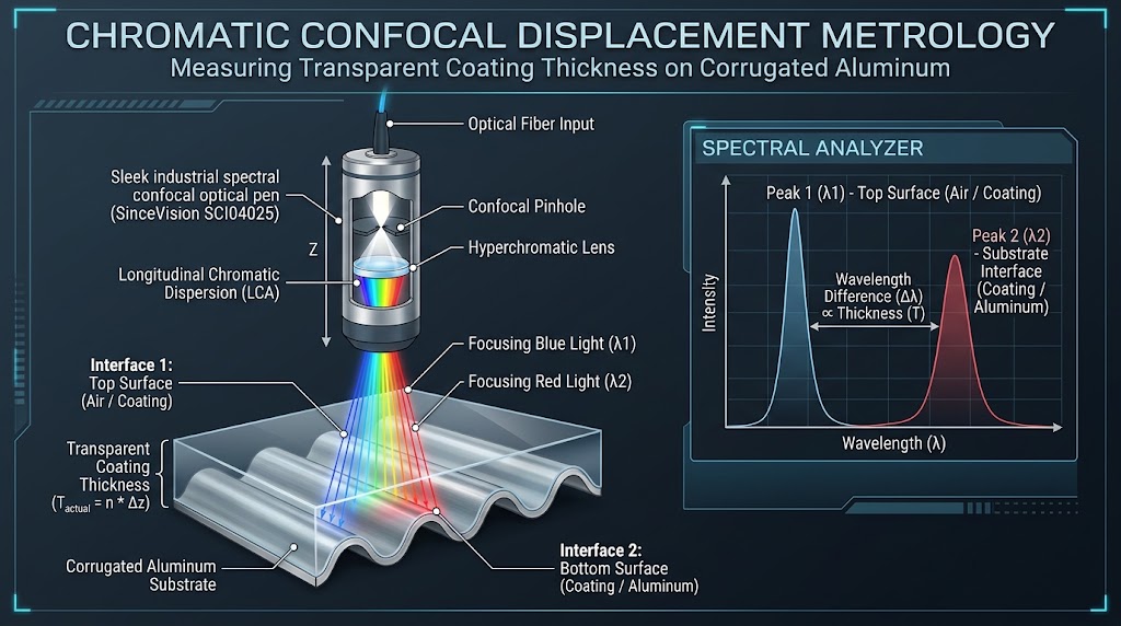
Image: Technical diagram explaining chromatic confocal metrology
The Spectral Confocal Measurement Principle
The SinceVision SCI04025 uses an optical pen containing specialized dispersive lenses that focus each wavelength of light at a different distance from the probe tip along the optical axis.
When the projected beam strikes a coated water-cooled plate:
Top Surface Reflection (Peak 1): The air-to-coating boundary reflects the specific wavelength focused at that exact height.
Bottom Surface Reflection (Peak 2): Light penetrating the transparent medium reflects off the coating-to-aluminum boundary at a longer focal wavelength.
Both reflected wavelengths return coaxially through the optical pen and pass through a confocal pinhole aperture. This pinhole mechanically blocks all out-of-focus light, ensuring that only the wavelengths matching the exact boundary depths reach the internal spectrometer detector.
The spectrometer captures two distinct spectral intensity peaks:
Peak 1 encodes the absolute Z-elevation of the outer coating surface.
Peak 2 encodes the position of the underlying aluminum plate.
Calculating Physical Coating Thickness
The distance between the two spectral peaks corresponds to the apparent optical thickness (T_optical). Inside the coating, light travels slower than in air according to the material's refractive index (n).
The controller calculates the true physical thickness (T_actual) using the calibrated formula:
T_actual = T_optical / n_group
Where:
T_actual is the true physical layer thickness.
T_optical is the uncompensated optical separation determined from sensor calibration.
n_group is the refractive index of the transparent or translucent coating material.
By capturing height data from both surfaces in a single measurement pass, the SCI04025 provides the verified data required to confirm that the coating satisfies design specifications.
Key Engineering Advantages of the SinceVision SCI04025
High-Precision Measurement: With a linearity of ±0.8 μm and a static measurement repeatability of 0.06 μm, the sensor delivers the dimensional accuracy needed for tight quality control tolerances.
Transparent Material Recognition: A minimum measurable thickness threshold of 130 μm allows reliable separation of top and bottom reflection peaks on transparent and translucent industrial coatings.
Non-Contact Detection: The optical sensing principle eliminates all physical contact with the workpiece, preventing scratches, deformation, or wear on delicate insulating layers.
Flexible Station Adaptation: An optical working distance (standoff) of 16 mm provides mechanical clearance for automated multi-axis scanning gantries and robotic inspection cells.

Step-by-Step Inline Inspection Workflow
Station Positioning: Mount the SinceVision SCI04025 sensor head at its 16 mm nominal working distance above the corrugated plate.
Material Index Input: Configure the sensor controller with the group refractive index (n) corresponding to the specific coating formulation.
Automated Surface Scan: Traverse the sensor along the corrugated channel paths via an automated motion stage.
Dual Peak Extraction: The high-speed spectrometer continuously isolates the top surface reflection (Peak 1) and bottom substrate reflection (Peak 2).
Simultaneous Profile Output: The controller records the 3D surface topography of the corrugated channel while calculating real-time coating thickness.
Tolerance Verification: The system automatically flags any region where coating thickness falls below electrical breakdown limits or exceeds thermal resistance limits.
3. Various Inspection Scenarios
Because spectral confocal technology isolates boundary reflections based purely on optical wavelength dispersion and spatial filtering, its capabilities extend across multiple high-precision industries. The SinceVision SCI04025 performs non-contact thickness, air gap, and surface topography metrology on semiconductor wafers, consumer electronic modules, optical glass components, and complex curved workpieces.
| Industry / Application Sector | Target Inspection Tasks & Features |
| 1. Semiconductor Industry | • Wafer thickness measurement • Precision micro-structure inspection |
| 2. Consumer Electronics Industry | • Camera-related structure distance measurement • Transparent cover thickness inspection |
| 3. Optical Manufacturing Industry | • Optical glass thickness measurement • Transparent substrate verification |
| 4. Complex-Shaped Workpieces | • Curved surface and chamfer profiling • Irregular structures measured at tilted angles |
1. Semiconductor Industry
Wafer Thickness Measurement: Measures absolute substrate thickness and thickness uniformity on silicon and compound semiconductor wafers.
Precision Structure Metrology: Evaluates surface steps, etched trenches, and functional thin-film layers without mechanical contact.
2. Consumer Electronics Industry
Camera-Related Structure Distance Measurement: Inspects miniature air gaps, lens spacing, and structural positioning within compact camera modules.
Transparent Cover Thickness Inspection: Profiles display cover glass, smart device lenses, and protective optical coatings to detect local thinning or surface distortion.
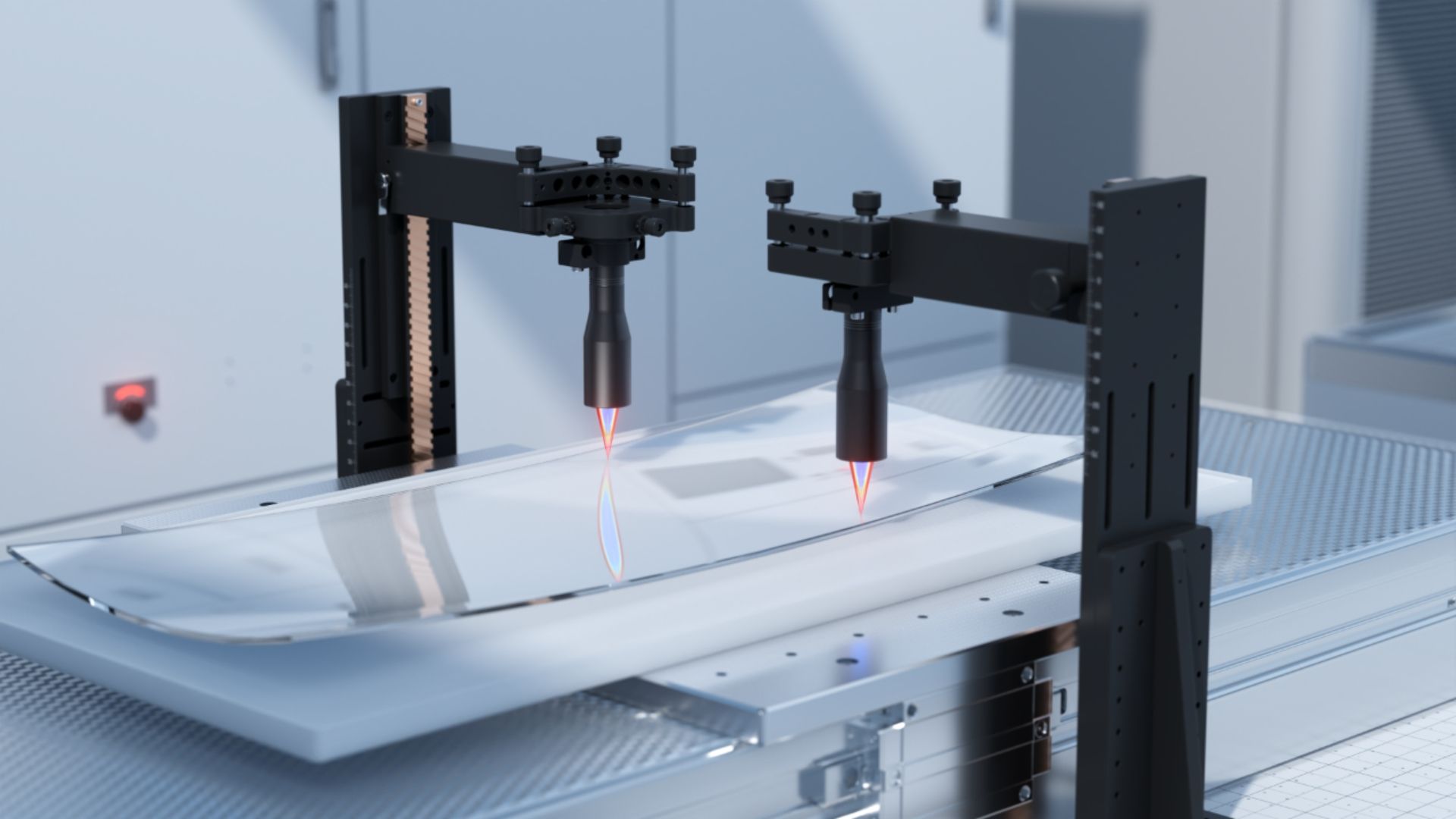
Image: Warpage inspection of a Car center console display glass panel
3. Optical Manufacturing Industry
Optical Glass and Transparent Substrate Measurement: Delivers sub-micron thickness and parallelism verification on polished glass plates, wafers, and flat panels.
Optical Component Quality Control: Inspects prisms, optical filters, and coated components, verifying physical dimensions and surface profiles without risk of scratching optical finishes.
4. Complex-Shaped and Curved Workpieces
Curved and Irregular Geometries: Measures parts with variable surface radii, bevels, and steep transition zones.
Angular Characteristic Adaptation: By leveraging the sensor's optical acceptance angle, the SCI04025 maintains reliable signal return on tilted surfaces, enabling continuous scanning across complex geometric shapes under production conditions.
Frequently Asked Questions (FAQs)
1. How does the SinceVision SCI04025 measure both surface shape and coating thickness at the same time?
The sensor uses longitudinal chromatic dispersion to separate white light into different wavelengths along the vertical axis. When the light strikes a transparent coating, reflections occur at both the top surface and the bottom substrate. Both reflected wavelengths travel back through a confocal pinhole to a spectrometer. The spectrometer detects two distinct intensity peaks: the first peak identifies the outer surface height to map 3D shape, while the difference between the two peaks determines the coating thickness.
2. Why is non-contact optical inspection critical for EV water-cooled plates?
Dielectric coatings on water-cooled plates are sensitive polymer layers. Traditional contact gauges or stylus indicators apply localized pressure that can scratch, indent, or tear the coating. Any physical defect reduces dielectric insulation resistance and can cause electrical arcing during high-voltage battery operation. The SinceVision SCI04025 operates at a 16 mm standoff distance, eliminating all contact risk.
3. What is the minimum transparent thickness the SCI04025 can measure?
The minimum measurable thickness for transparent objects on the SinceVision SCI04025 is 130 μm. This limit is governed by the optical spectral width of the reflection peaks on the spectrometer array. If a transparent layer is thinner than 130 μm, the reflection peaks from the upper and lower surfaces overlap on the detector, preventing accurate separation.
4. How does the sensor handle corrugated channels and curved surfaces without losing measurement signal?
The SCI04025 optical pen is engineered with a wide optical acceptance angle. On diffuse or semi-translucent coatings, light scatters across multiple angles, allowing the coaxial lens to capture sufficient light even on tilted channel slopes. In addition, the 16 mm working distance provides ample physical clearance to scan over channel crests and valleys without mechanical interference.
5. Why must refractive index compensation be applied to transparent thickness measurements?
The sensor's internal calibration table calculates distance assuming light travels through air (n ≈ 1.0). When light enters a transparent coating with a higher refractive index (typically n = 1.4 to 1.6 for industrial polymers), the speed of light decreases, shifting the apparent focal position deeper. To find the true physical thickness, the measured optical thickness must be divided by the material's refractive index using the formula T_actual = T_optical / n.

Featured Sensor
SCI04025
You can also read
Unlocking Flame Cellular Instability: Advanced High-Speed Camera Flame Imaging with the SinceVision SH8 Series
Oct 09, 2026
Analyzing Brittle Fracture in Tomato Roots: A SinceVision High-Speed Camera & DIC Experiment for Agricultural Robotics
Sep 01, 2026
3D Laser Profiler for Lithium-Ion Battery Top Cover Bonding Height Measurement
Aug 14, 2026
Observation of Embryonic Fibroblasts with sCMOS Camera for Multichannel Imaging
Jun 23, 2026
Automating Automotive Body Gap Detection with the SinceVision SR8060H 3D Laser Profiler
Jun 05, 2026



 Compare
 Clear the comparison bar

