


13th Semiconductor Equipment, Core Components, and Materials Expo | SinceVision to Showcase Advanced Semiconductor Measurement Solutions
SinceVision will present semiconductor precision measurement solutions, including solder ball inspection, wafer edge alignment, and wafer thickness detection, at the 13th Semiconductor Equipment, Core Components, and Materials Expo in Wuxi.
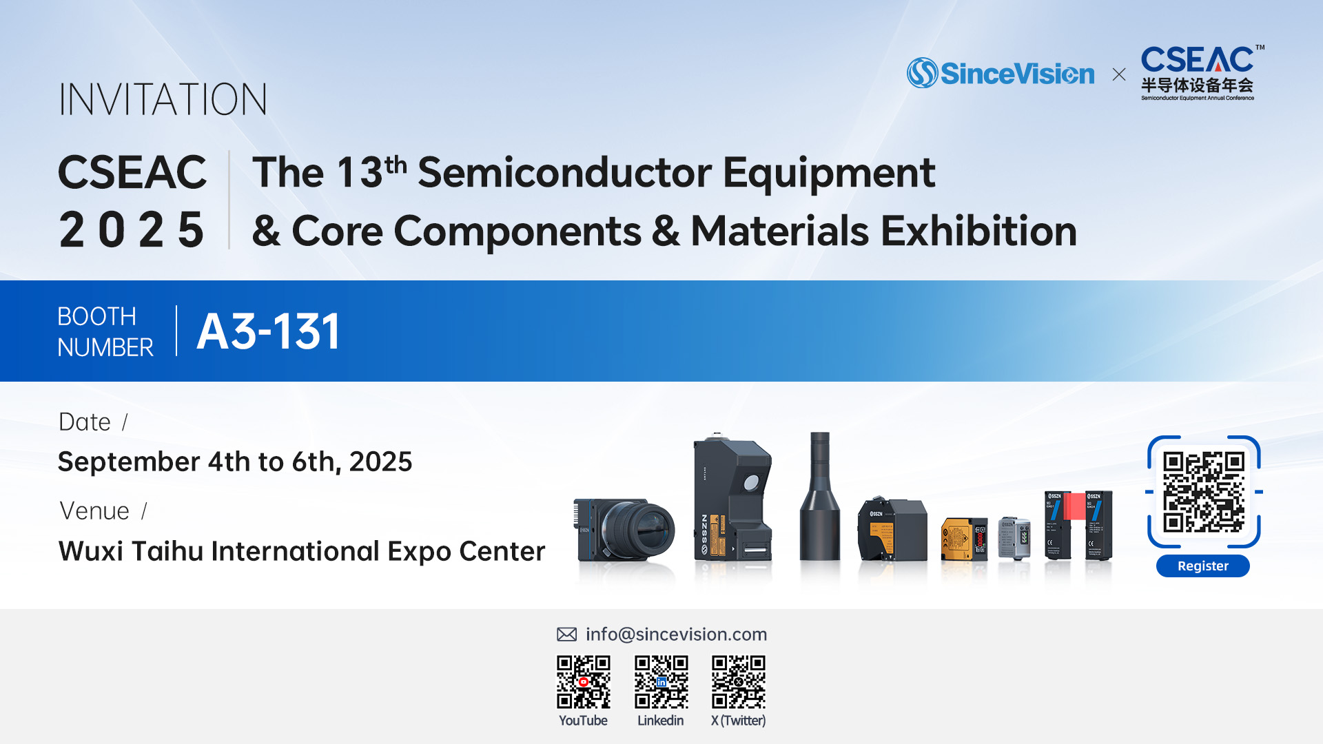


Wuxi, China – September 1, 2025 – SinceVision, a pioneer in industrial sensor innovation, will participate in the 13th Semiconductor Equipment, Core Components, and Materials Expo (CSEAC) at the Wuxi Taihu International Expo Center. At booth A3-131, the company will present its full range of products and precision semiconductor measurement solutions designed to drive the intelligent transformation of semiconductor manufacturing.
As a leader in precision sensing and inspection, SinceVision will demonstrate its classic semiconductor application cases and cutting-edge 3D measurement technologies. The company’s solutions are engineered to deliver accuracy, stability, and speed for semiconductor inspection and production processes.

Featured Applications at the Expo
Chip Solder Ball Height Inspection
Overcomes solder ball reflection interference for reliable results.
One-click indexing for faster and easier operation.
Key specs: Line width 14.5 mm, depth of field 5.2 mm, X spacing 5 μm.
Linearity ±0.02% F.S., frame rate 3200–67000 Hz.

Wafer Edge Alignment
Stable detection of transparent and semi-transparent materials.
High-precision alignment with repeat accuracy of 5 μm.
Key specs: Measurement range 10 mm, frame rate 4000 Hz.
Center deviation ±0.05 mm, angle deviation ±0.1°.

Wafer Thickness Measurement
Thickness accuracy up to 1 μm with temperature drift<0.015% F.S./°C.
Stable through-beam measurement with no offset.
Key specs: Range 1 mm, minimum thickness 30 μm.
Sampling frequency 500–33000 Hz.

Meeting Industry Partners
SinceVision looks forward to engaging with industry professionals and partners at the event. Visitors are invited to discuss future paths for semiconductor manufacturing upgrades, explore new opportunities for high-quality industrial transformation, and experience hands-on demonstrations of SinceVision’s semiconductor solutions.
Event Information
Event: 13th Semiconductor Equipment, Core Components, and Materials Expo
Date: September 4–6, 2025
Location: Wuxi Taihu International Expo Center
Booth: A3-131
SinceVision welcomes all semiconductor industry peers and partners to visit the booth and explore cutting-edge sensing technologies that ensure precision, efficiency, and innovation in semiconductor production.
Book a meeting at info@sincevision.com or click here to receive a ticket.

You can also read
How SinceVision High-Speed Cameras Power Electrospinning Research at Zhejiang Sci-Tech University (ZSTU)
Jul 01, 2026
SinceVision's New SD33-300 and SD33-600: Long-Range Laser Displacement Sensors for Wide-Span Precision Measurement
May 09, 2026
Research Published in Nature Communications: SinceVision Camera Validates New Neuromorphic Imaging Array
Apr 22, 2026
SinceVision and Lunitek Announce Partnership to Advance Scientific Discovery in Italy
Apr 21, 2026
SinceVision Launches New Back-Illuminated Cooled sCMOS Camera Series for Ultra-Low-Light Scientific Imaging
Nov 17, 2025


 Compare
 Clear the comparison bar
