


Applications of 3D Laser Profilers in Silicon Wafer Manufacturing | SinceVision
SinceVision has established itself as a leader in cutting-edge sensor technology, particularly in the realm of 3D laser profilers. These advanced measuring instruments play a crucial role in various manufacturing processes, especially within the photovoltaic (PV) industry. This article will delve into the diverse applications of SinceVision's 3D laser profilers, highlighting their significance in ensuring quality control and precision measurement in solar cell production.
Applications in Silicon Wafer Manufacturing
1. Wafer Thickness, Line Mark, and TTV Detection
a. Application Scenario
After the silicon wafer is produced, it needs to be tested by a sorting machine for multiple indicators such as thickness, linear marks, TTV, warpage, etc. to determine whether the silicon wafer meets the set requirements, and then sorted into the corresponding bin box according to the test data, and finally the silicon wafer is sorted into different grades.

Fig: Silicon wafer thickness/line mark/TTV detection
b. Solution
The SR8010 3D laser profiler measuring instrument can perform thickness, TTV, maximum line mark and other tests on various special silicon wafers. The repeatability of the thickness of the measurement items can be within 0.5um, the repeatability of TTV within 1.5um, and the repeatability of line marks within 1.5um. It has ultra-high-profile points and detection speed and can achieve accurate and efficient detection.
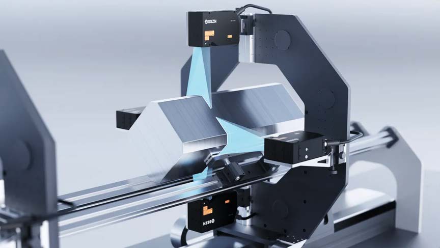
2. Silicon rod size detection
a. Application Scenario
Silicon rods are widely used in the field of solar cell manufacturing due to their excellent performance. After the silicon rods are manufactured, they may have defects such as external cracks, voids, bubbles, internal impurities, etc., so strict quality control tests are required before they can be used in subsequent production

Fig: Silicon rod size detection
b. Solution
The SR7060 3D laser profiler measuring instrument can detect multiple items such as size, arc length, verticality, etc. of silicon rods. It uses multiple measuring instruments to scan and adopts image algorithm stitching technology to form a complete image of the silicon rod, with an item accuracy of 0.02mm.
You can also read
SinceVision Launches SH8 Series Ultra-High-Speed Cameras: Capturing Every Instant of High-Speed Action at 1.10 million fps
Jun 09, 2026
SinceVision Launches Solis B0555 PRO sCMOS Camera for Ultra-Low-Light Single-Photon Imaging
May 12, 2026
SinceVision's New SD33-300 and SD33-600: Long-Range Laser Displacement Sensors for Wide-Span Precision Measurement
May 09, 2026
Research Published in Nature Communications: SinceVision Camera Validates New Neuromorphic Imaging Array
Apr 22, 2026
SinceVision and Lunitek Announce Partnership to Advance Scientific Discovery in Italy
Apr 21, 2026


 Compare
 Clear the comparison bar
