









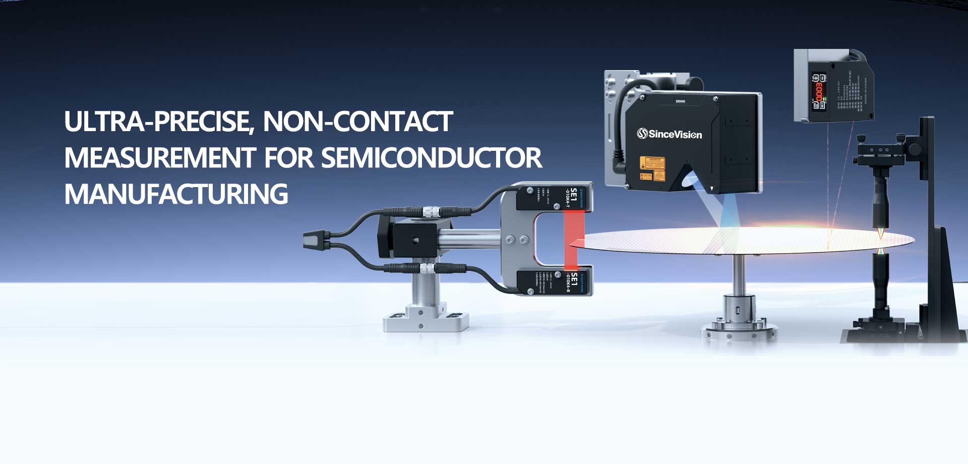
Precision Measurement for Every Stage of Semiconductor Manufacturing
Eliminate contact damage, improve yield rates, and achieve sub micron accuracy from bare wafer inspection to final chip packaging.
-
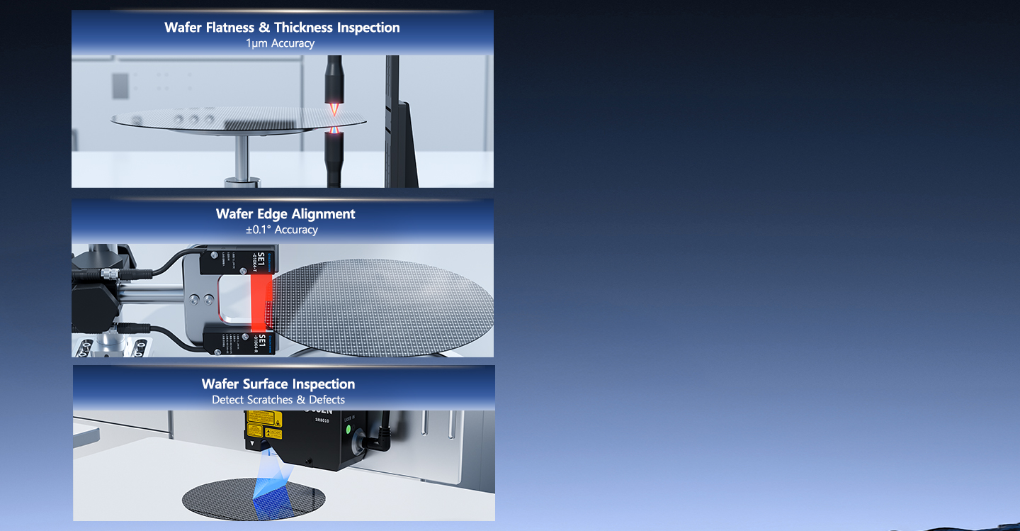
Wafer Manufacturing
Sub micron flatness, thickness, and surface quality control for bare and patterned wafers.
Ensure strict geometric tolerances before front end fabrication begins. SinceVision spectral confocal and optical edge sensors deliver high speed, non contact measurement on reflective, transparent, and dark silicon surfaces without risking micro scratches or contamination.
Key Applications:
1. Wafer Flatness & Thickness Inspection: Achieve 1µm accuracy using dual probe non contact measurement to detect warpage and total thickness variation.
2. Wafer Edge Alignment: Maintain ±0.1° alignment accuracy with optical edge sensors for reliable wafer centering and notch detection.
3. Wafer Surface Inspection: Capture high resolution surface profiles to identify micro scratches, pits, and particle defects early in production. -
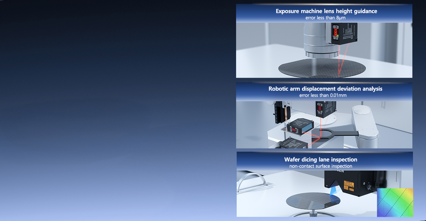
Wafer Processing
Real time positioning and surface monitoring for lithography, handling, and dicing.
Maintain micron level repeatability across high speed wafer handling and fabrication equipment. SinceVision laser displacement sensors provide stable, real time feedback to keep robotic transfers, exposure lenses, and dicing lines operating within tight process windows.
Key Applications:
1. Exposure Machine Lens Height Guidance: Keep focus positioning error under 8µm for consistent lithography alignment.
2. Robotic Arm Displacement Deviation Analysis: Track multi axis transfer stability with under 0.01mm error to prevent wafer collision or drop.
3. Wafer Dicing Lane Inspection: Perform fast, non contact surface inspection along kerf lines to catch chipping and delamination immediately after dicing. -
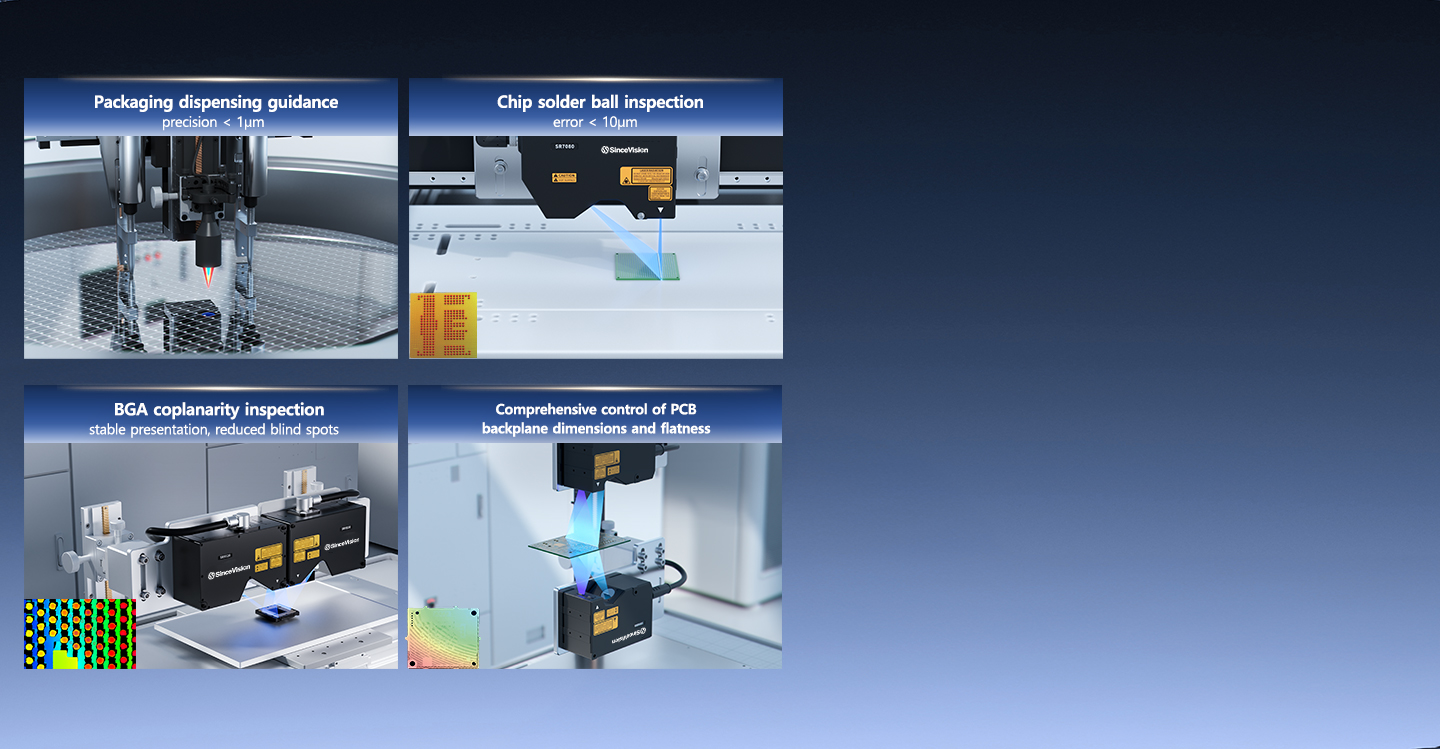
Chip Packaging
High speed 3D profiling for dispensing, solder balls, BGA coplanarity, and PCB substrates.
Verify interconnect integrity and substrate flatness at full line speed. Powered by the 3D laser profiler and spectral confocal sensors, SinceVision systems reduce blind spots on reflective solder joints and complex IC substrates.
Key Applications:
1. Packaging Dispensing Guidance: Guide adhesive and encapsulant dispensing paths with precision under 1µm.
2. Chip Solder Ball Inspection: Measure solder ball height, volume, and missing bumps with error under 10µm.
3. BGA Coplanarity Inspection: Deliver stable 3D imaging with reduced blind spots across dense ball grid arrays.
4. PCB Backplane Control: Monitor overall substrate dimensions, warpage, and flatness across the entire backplane. -
-


Get Your Free Application Guide
To log in to the official website of SinceVision,
please fill in the registration information
Membership Service
Real-world inspection cases
Recommended measurement solutions
Key technologies and performance advantages


 Compare
 Clear the comparison bar

