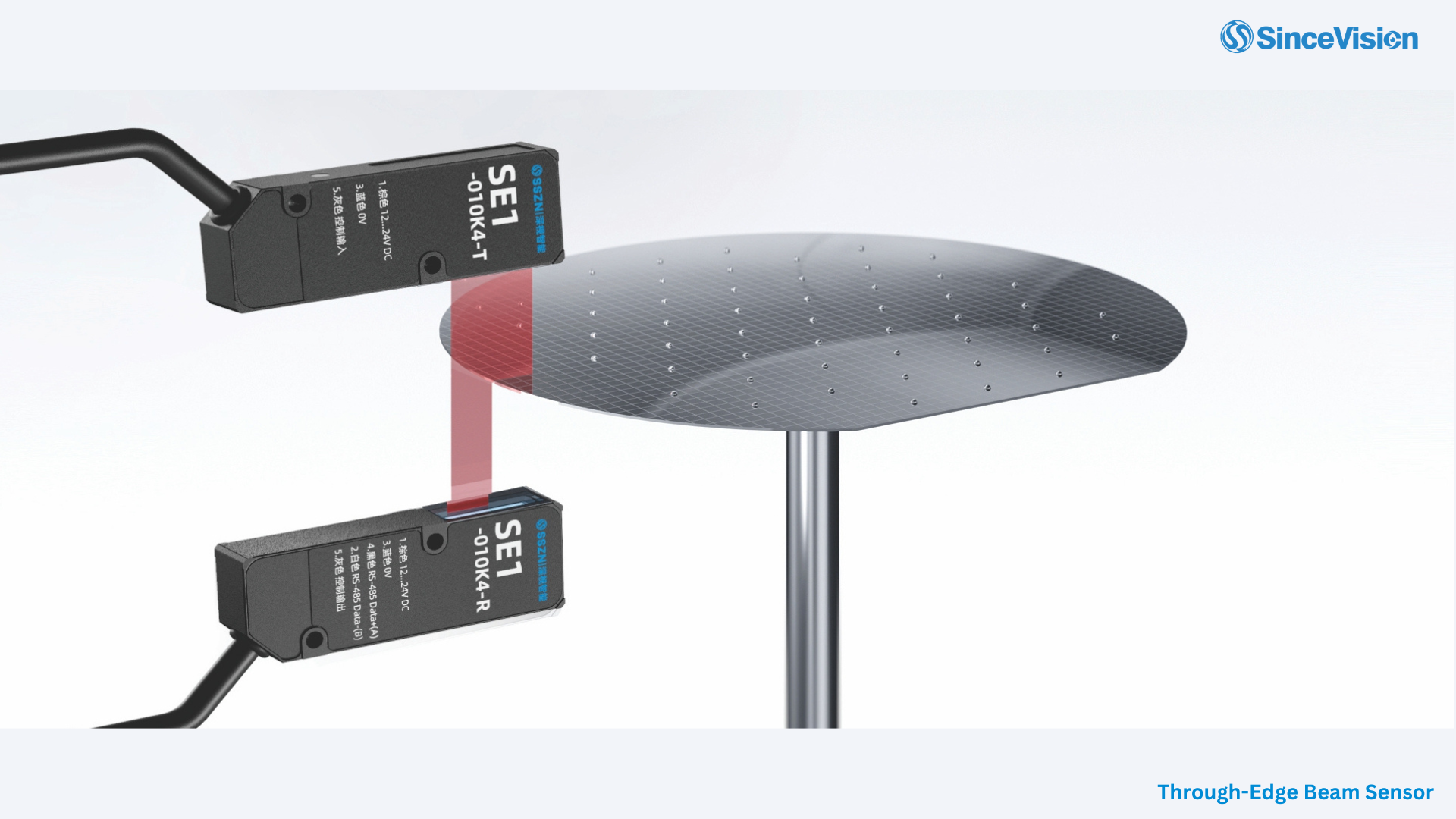
In the chip packaging testing phase, accurate detection of wafer concentricity and notch positioning is critical for improving the accuracy of wafer cutting. Proper alignment of the wafer center and notch position directly influences the yield of chip production, making it essential to implement effective measurement solutions. This article discusses the challenges associated with wafer concentricity and notch detection and presents a reliable solution using SinceVision's high-precision edge measurement sensors.
Application Scenario
During the chip packaging process, wafers must be precisely centered and aligned to ensure successful cutting and placement of chips. The concentricity of the wafer and the position of the notch must be accurately detected to enhance cutting precision and minimize waste. Any misalignment can lead to defective chips, resulting in increased production costs and reduced yield.

Solution: SinceVision's SE1 Series Sensors
To effectively address these challenges, SinceVision recommends the use of the SE1 series high-precision edge measurement sensors. These sensors are designed to be installed opposite each other for through-beam measurement at the edge of the wafer.
The key features of the SE1 series include:
a. Real-Time Measurement: The sensors continuously monitor the wafer's position as it rotates, calculating the center position of the circle based on measurement data.
b. Accurate Centering: Once the center of the wafer is determined, a robotic arm or actuator moves the wafer to align it with the rotation axis, ensuring precise cutting.
c. Notch Positioning: After aligning the wafer's center, the sensors facilitate the detection of the notch position. The actuator then rotates the wafer to the specified angle for accurate processing.
Benefits of Using SE1 Series Sensors
1. High Precision: The SE1 series sensors provide exceptional accuracy in detecting wafer concentricity and notch positioning, significantly enhancing production quality.
2. Rapid Response: With fast measurement capabilities, the sensors enable quick adjustments during the production process, reducing downtime and improving efficiency.
3. Robust Performance: Designed for high-speed applications, the SE1 series sensors maintain reliable performance even in challenging manufacturing environments.
Conclusion
Implementing SinceVision's SE1 series high-precision edge measurement sensors in the chip packaging testing phase significantly improves wafer concentricity and notch detection. By ensuring accurate positioning, manufacturers can enhance cutting precision, increase yield, and reduce production costs. As the demand for high-quality chips continues to rise, leveraging advanced sensor technology will be key to maintaining a competitive edge in the semiconductor industry.
For more information on SinceVision's sensor solutions and how they can optimize your production processes, please reach out to us.
-
Exhibition2026-03-09AW2026 Seoul Recap: Ten Live Demos, the Future of Manufacturing, & South Korea
-
Industry News2026-02-13Automotive Connector Pin Inspection: How 3D Blue Laser Profiling Achieves Sub-0.01mm Repeatability
-
Corporate News2026-02-10Holiday Notice: Chinese New Year & Spring Festival 2026
-
Corporate News2026-02-04SinceVision to Showcase Advanced 3D Sensing and High-Speed Imaging Solutions at SPS Guangzhou 2026


