


 Chip Inspection with SinceVision 3D Laser Profiler")
Ball Grid Array (BGA) Chip Inspection with SinceVision 3D Laser Profiler
Ball Grid Array (BGA) is one of the most common packaging methods for chips. The solder balls in BGA packages act as connection points between chips and circuit boards, directly impacting the contact quality between terminals and PCB lines, and thus influencing the overall quality of BGA chips. With the miniaturization of products and the increase in functionality, requirements for solder ball parameters like height and flatness have become increasingly stringent. To address potential defects caused by inconsistencies in solder ball height resulting from production errors, SinceVision leverages high-precision line laser products to conduct yield analysis and inspection of chip solder balls, ensuring superior product quality.
BGA chip packaging relies on solder balls to connect chips and circuit boards. However, as miniaturization and functional integration advance, challenges arise:
Solder Ball Height & Flatness: Variations in height and uneven surfaces can lead to poor electrical connections and compromised chip reliability.
Defect Detection: Identifying defects like missing, deformed, or misaligned solder balls is critical for ensuring high manufacturing standards.
Increased Precision Demands: Rising functional complexity of chips necessitates advanced inspection tools to meet stringent production tolerances.
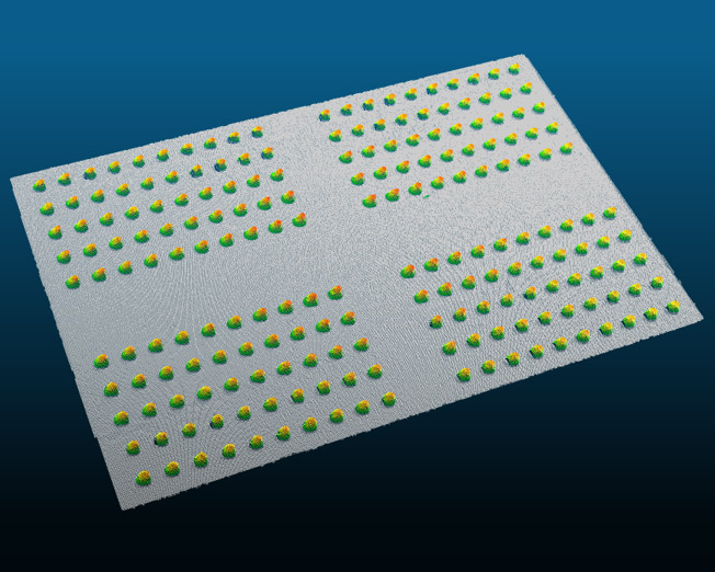
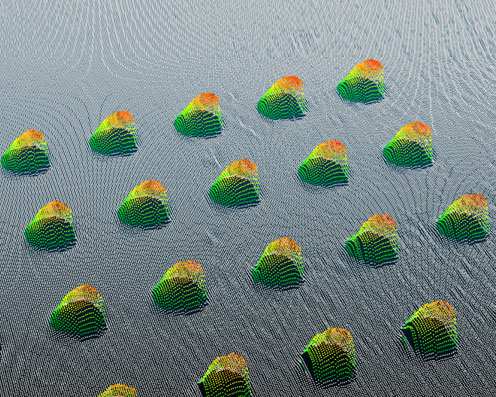
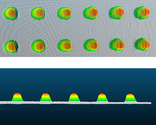
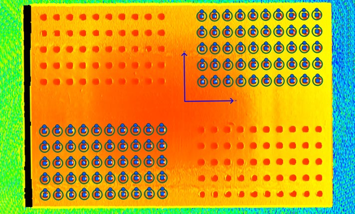
Imaging Effect Picture
Inspection Parameters


SinceVision Solution: SR8060 3D Laser Profiler
Camera Selection
| Model number | SR8060 | |||
| Reference distance (CD) | 60mm | |||
| Measuring range | Z-axis height (FS) | 18mm | ||
| X-axis width | Near side | 26mm | ||
| Reference distance | 31mm | |||
| Remote side | 36mm | |||
| Light source | Light source wavelength | 405nm blue light | ||
| Laser class | 2M | |||
| Laser output power | 10mW | |||
| Repetition accuracy | Z-axis (height) | 0.2μm | ||
| X-axis (width) | 5μm | |||
| linearity | Z-axis (height) | ±0.02% of F.S. | ||
| Contour data interval | X-axis (width) | 12μm | ||
| X-axis contour points | 3200 | |||
| Reflection Angle (°) | 33 | |||
| Scanning speed (Hz) | 3200 ~ 67000 | |||
| Dimension (mm) | 124.5×84×55. 2 | |||
| Weight (g) | 630 | |||
| Temperature characteristic | 0.02% F.S./℃ | |||
| Encoder input | Single-ended, differential encoder is supported | |||
| Input/output | One 100Base-TX/1000Base-T Ethernet interface | |||
| Operation Temperature | 0~50℃ | |||
| Storage Temperature | -20~70℃ | |||
| Working humidity | 35% to 85% without condensation | |||
| ESD Protection | Contact discharge 4kV, air discharge 8kV, in accordance with IEC 61000-4-2 standards | |||
| EFT protection | Power port 2kV/5 or 100kHz, signal port 1kV/5 or 100kHz, in accordance with IEC 61000-4-4 standards | |||
| Impact | 50Gs/3ms per axis, in accordance with IEC 68-2-27 Ea standard | |||
| Vibration | 10Gs (10-500Hz), compliant with IEC 68-2-6 Fc standard | |||
| degrees of protection provided by enclosure | IP67, in accordance with IEC 60529 standard | |||